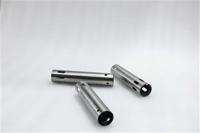
As semiconductor manufacturing evolves to higher and more complex processes, small differences in material properties often determine the upper limit of chip yield and equipment stability. Niobium (Nb), as a rare metal with high melting point, corrosion resistance, low outgassing rate, and superconducting properties, is becoming one of the indispensable key materials in high-end semiconductor equipment by virtue of its unique advantages. Among them, niobium processed parts, represented by V-shaped groove blocks and precision components with mounting holes, play an irreplaceable role in many core process links.
In semiconductor manufacturing, processes such as wafer heat treatment, annealing after ion implantation, and diffusion often need to be performed at temperatures of 800°C-1200°C or even higher, and have almost stringent requirements for wafer positioning accuracy and environmental purity. Traditional stainless steel and ceramic materials are prone to deformation and release impurities at high temperatures, making it difficult to adapt to the needs of high-end manufacturing processes. Niobium processed parts perfectly solve this pain point.
The melting point of niobium is as high as 2468°C, and it can still maintain excellent structural strength and an extremely low thermal expansion coefficient (about 7.3×10⁻⁶/°C) at high temperatures, which means that the V-groove wafer clamp made of niobium will not undergo significant deformation due to thermal expansion and contraction during repeated high-temperature cycles. The V-shaped groove structure can accurately fit the edge of the wafer, achieve micron-level positioning accuracy, and avoid uneven heating caused by wafer deflection in high-temperature processes, thus ensuring the uniformity of wafer surface doping, oxidation, and other processes. At the same time, niobium is chemically stable at high temperatures and does not react with silicon, oxygen, or most process gases. It does not release metal impurities to the wafer surface, which greatly reduces the risk of process contamination. It has become a core component for wafer loading and positioning in high-temperature diffusion furnaces and rapid thermal processing (RTP) equipment.
Plasma processes such as dry etching, physical vapor deposition (PVD), chemical vapor deposition (CVD), etc., are key links in achieving pattern transfer and film growth in the semiconductor chip manufacturing process. This type of process relies on a high-energy plasma environment. The components inside the chamber not only need to withstand the continuous bombardment of the plasma, but also need to withstand the erosion of corrosive process gases such as fluorine-based and chlorine-based, while avoiding the release of impurity ions to contaminate the wafer.
Niobium's corrosion resistance to fluorine and chlorine plasma is far superior to traditional materials such as stainless steel and aluminum alloys. It can effectively resist corrosion and sputtering in plasma environments and reduce particle pollution caused by component loss. Therefore, niobium processed parts are often used as electrode supports, plasma shields, edge ring components, etc., in the chamber. On the one hand, these components can optimize the electric field and airflow distribution in the chamber, improve the uniformity of the plasma, and thereby ensure the consistency of the etching and deposition processes; on the other hand, the low sputtering rate characteristics of niobium can significantly reduce the migration of metal impurities to the wafer surface, reduce film defects, and provide guarantee for the yield of advanced process chips. In addition, the high vacuum compatibility of niobium material allows it to have an extremely low outgassing rate in a high vacuum chamber environment. The released gas will not affect the vacuum degree of the chamber, ensuring the stable operation of the plasma process.
With the development of cutting-edge semiconductor technologies such as superconducting quantum devices, low-temperature CMOS, and low-temperature detectors, the process environment extends to extremely low temperatures and high vacuum, posing new challenges to the low-temperature performance of component materials. The superconducting critical temperature of niobium is about 9.2K. It can show excellent superconducting properties in the liquid helium temperature range (4.2K). At the same time, it can still maintain good mechanical properties in extremely low temperature environments without the risk of brittle fracture, making it an ideal material for low-temperature semiconductor process equipment.
In the preparation and testing equipment of superconducting quantum devices, niobium processed parts are often used as fixing parts, thermal conductive parts, and electrode components in low-temperature chambers. Its stable low-temperature dimensional characteristics can ensure that components do not deform during repeated temperature rise and cooling processes, maintaining the precise positioning of the device and chamber; the extremely low gas release rate can avoid gas adsorption and release in low-temperature environments and ensure high vacuum in the chamber. At the same time, niobium superconducting components can reduce energy loss in low-temperature environments, improve the signal transmission efficiency of the device, and provide key support for the research and development and mass production of superconducting semiconductor technology.
lisa
Sales Manager
Phone Number/weChat/whatsApp
(82)-18291772322
Ta-Nb@titanmsgp.com