

Niobium Disc Targets

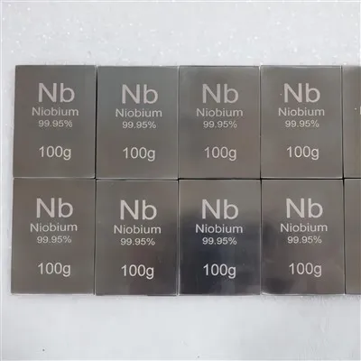
In modern semiconductor wafer manufacturing, superconducting quantum device research and development, precision optical coating, and physical vapor deposition (PVD/magnetron sputtering) of new energy photovoltaic cells, the purity of the target, internal grain size distribution, and surface flatness It directly determines the uniformity, adhesion and electrical/optical properties of thin film deposition. When conventional metal targets are powerless in the face of high-power sputtering, extreme superconducting critical temperature requirements, or precision optical refractive index regulation, the special refractory metal Niobium (Niobium) has shown an irreplaceable core value. As shown in the physical picture of the product, the High-Purity Niobium Sputtering Targets/Planar Nb Disc Targets (High-Purity Niobium Sputtering Targets/Planar Nb Disc Targets) professionally presented by us are precisely for the world's cutting-edge thin film deposition and vacuum coating The flagship product created by engineering experts for the stringent requirements of ultra-pure materials, micron size tolerances and extreme sputtering stability.
As a key member of the refractory metal family, niobium (Nb) not only has a melting point of up to 2477 °C, a dense structure of 8.57 g/cm ³ and excellent corrosion resistance, but also enjoys the reputation of "the cornerstone of superconductivity" in the field of low-temperature physics (Its superconducting critical temperature under normal pressure is as high as 9.25 K, which is the highest among all pure metal elements). At the same time, in the field of optical coatings, niobium pentoxide (Nb ₂ O You) thin films have extremely high refractive index and extremely low light absorption loss, making them an indispensable core material for modern precision optical filters and anti-reflection films. It can be clearly seen from the physical drawing of the product that our niobium round target has been processed by precision turning and surface grinding, and the surface presents a delicate and uniform radial metal turning luster without any pores, scratches, oxide scales or edge collapses. For European and American thin film technology purchasers and process engineers who pay attention to film yield, sputtering rate stability and batch consistency, choosing a high-purity niobium sputtering round target means locking a high standard guarantee for the entire PVD coating production line.
In the process of manufacturing and microstructure control, we strictly select high-purity electrolytic niobium or electron beam smelting (EBM) niobium ingots (purity can reach 99.95% 3N5 to 99.995% 4N5), and completely remove trace impurities such as tantalum (Ta), iron (Fe), oxygen (O), nitrogen (N), and carbon (C) that affect the stability of the sputtering plasma and the electrical properties of the film. Aiming at the most concerned pain point of "grain size and orientation homogeneity" in the process of magnetron sputtering, we adopt a unique multi-directional hot forging and cross-rolling process, and precisely control the high-vacuum recrystallization annealing temperature to reduce the internal average of the target The grain size is stably controlled below 50 µ m to 100 µ m to ensure that the grain structure is fine and isotropic. This uniform microstructure can significantly Arcing/Particle Generation in the sputtering process, ensuring the thickness uniformity and compactness of the deposited film. Before leaving the factory, each target material has undergone 100% ultrasonic flaw detection (UT) to detect internal defects, and has been cleaned without ultrasonic oil and packed with vacuum moisture-proof.
In order to facilitate the global coating process team, R&D laboratory and supply chain management manager to conduct project evaluation and specification matching, we have sorted out the core technical parameters and specifications of this series of niobium round targets as follows:
Table of Core Parameters and Technical Specifications
| Property | Value | Advantages |
| Product Name | High-Purity Niobium Sputtering Targets/Nb Disc Targets | Core targets designed for magnetron sputtering (PVD), electron beam evaporation and superconducting/optical thin film deposition |
| Grade | RO4200-1/RO4210-2 (industrial and high-purity sputtering grade pure niobium) | Very low impurity content, fine and uniform internal grains, dense sputtering film and no abnormal discharge |
| Purity | ≥ 99.95% (3N5) / ≥ 99.99% (4N) / ≥ 99.995% (4N5) | Strictly control impurities such as Ta, O, N, C, H, etc. to ensure zero pollution of semiconductors and superconducting devices |
| Density | 8.57 g/cm ³ (close to 100% theoretical density) | No shrinkage holes, slag inclusions or microscopic holes in the interior, the target utilization rate is high, and the sputtering rate is stable |
| Melting Point | 2477 °C (4491 ° F) | Extremely high thermal resistance upper limit, able to withstand the thermal load of high power DC/RF magnetron sputtering |
| CTE | 7.3 × 10⁻⁶ / K (20–100℃) | Excellent thermal stability, and it is not easy to warp during sputtering heating and cooling cycles |
| Dimensions | Diameters: Ø 25.4 mm (1 ")-Ø 400 mm (16"); Thickness: 1.0 mm-25.0 mm Customized | Covering standard scientific bench sputtering instruments (such as 2-inch, 3-inch, 4-inch targets) and industrial-grade large-size production line specifications |
| Tolerance | Diameter tolerances: ± 0.05 mm-± 0.10 mm; Thickness tolerance: ± 0.05 mm; Surface roughness: Ra ≤ 0.8 µm | Precisely matched with various magnetron sputtering cathode gun heads to ensure good heat conduction and stability |
| Processing | Multiple electron beam melting (EBM) > Multi-directional hot forging > Cross rolling > Vacuum recrystallization annealing > CNC precision turning and flat grinding | Completely break the as-cast coarse grains, realize the homogenization of fine grains, and effectively suppress sputtering particles |
| Finish&Bonding | Precision turning glossy Finish/mirror Finish; Support oxygen-free copper backplane (OFHC Cu) Indium Bonding | Binding service is clean and oil-free, and provides an integrated backplane binding solution, which greatly improves heat dissipation efficiency and target life |
| Standards | ASTM B393 (Niobium and Niobium Alloy Strip, Sheet, and Plate) and internal control standards for semiconductor sputtering targets | Full compliance with European, American and international high-purity electronic materials manufacturing and control regulations |
| Deposition Method | DC Magnetron Sputtering, RF Sputtering and Reactive Sputtering | Not only directly deposit pure metal niobium conductive/superconducting layers, but also react with oxygen to deposit Nb₂O5 communicating optical film |
In-depth analysis of industry application and procurement value
In actual cutting-edge technology and industrial manufacturing scenarios, high-purity niobium circular targets have shown irreplaceable value. First of all, in the field of Superconducting Electronics and Quantum Computing (Superconducting Electronics & Quantum Computing), high-purity (4N and above) niobium targets are the core source materials for the preparation of Josephson Junctions, superconducting quantum interferometers (SQUID) and superconducting nanowire single-photon detectors (SNSPD). The extremely low gap gas impurities ensure that superconducting films have extremely high residual resistance ratio (RRR) and excellent superconducting transition properties. Secondly, in the field of precision optics and display coatings (Optical Coatings & Displays), niobium oxide thin films prepared by reactive magnetron sputtering are widely used in high-end lens antireflection coatings, AR/VR optical modules, high-power laser mirrors and touch screen vanishing layers because of their high refractive index, wide transparent band and excellent weather resistance. In addition, in advanced semiconductor manufacturing processes and photovoltaic cells, niobium thin films are also used as high-performance diffusion barriers and doped layers for transparent conductive oxides.
We are well aware of the stringent requirements of European and American B2B purchasers and scientific research institutions for target quality consistency, composition transparency and delivery safety. Each factory niobium round target is accompanied by the original material inspection report (MTC) that complies with the EN 10204 3.1 standard, including detailed glow discharge mass spectrometry (GDMS) total element impurity analysis, average grain size metallographic report, ultrasonic flaw detection (UT) qualification certificate and full inspection dimensional tolerance record. In terms of packaging and delivery, after the target material is ultrasonically cleaned and dried by ultra-pure water and anhydrous ethanol, it is double-sealed by independent vacuum nitrogen filling/vacuum moisture-proof aluminum foil bag, built-in high-density EPE pearl cotton suspension card groove is shockproof and isolated, and loaded into export grade Hard fumigation-free wooden box completely eliminates oxidation and bump damage in cross-border air or sea transportation. Whether you need single-piece small-size proofing in university scientific research laboratories, or batch specification procurement and one-stop customization of copper backplane binding in large vacuum coating factories, we can provide you with fast response and global worry-free supply Chain delivery guarantee.

Hot Tags: niobium disc targets, China niobium disc targets manufacturers, suppliers, factory