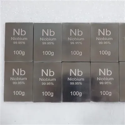

Products Advantages
Even grain structure, less banding, better yield
Grain size of 4N niobium targets bought from other sources varies significantly (100-300um) with random structure. Sputtering rate across the target surface varies significantly, creating banding of film thickness on substrates. This increases waste in large volume coating. Through cross rolling and directional annealing, grain size is controlled to between 25-45um, with a random, low intensity structure. Sputtering rate variation across a single target is very low (<5%). Substrate waste drops with it, and coating yields go up.
Fewer particles and fewer arcs
Inclusions in the form of O, N, C and H are a major cause of particle defects and frequent arcing within PVD systems. Excessive arcing may create pinholes in films and could damage expensive power supplies. By electron beam refining, we have very low levels of oxygen (<50ppm) and nitrogen (<30ppm). Very low levels of hard, brittle inclusions are achieved. During continuous high power sputtering operations, there is significantly less arcing. Fewer chamber openings, less maintenance, more hours on the tool.

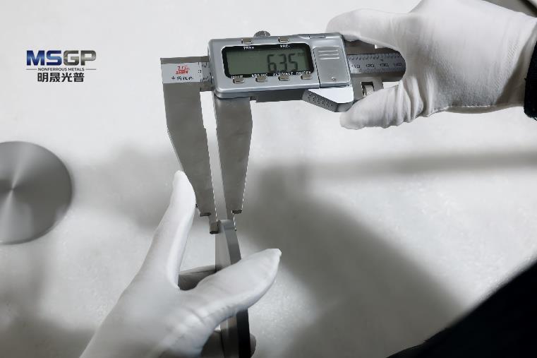
Tolerances tight enough for a 4 inch cathode
Overall diameter and thickness tolerances of +/- 0.1mm and +/-0.15mm respectively, along with rounded edges, will prevent cracking due to clamping. Targets bought from other generic sources often have larger tolerances meaning that gaps develop when installed. Run the system and heat parks in those gaps; the target distorts or the bond lets go. Both unbonded targets or copper backed targets can be supplied. Within a batch of bonded targets, thermal resistance variation is very small. Therefore in production, cooling parameters do not need to be frequently changed depending on the target supplied.
Microstructure data that keeps a coating process stable
Most suppliers only provide basic certificates of analysis. The files provided with each batch include grain size data, structure analysis and dimension data. In R&D laboratories and multiple chamber coating facilities, batches of targets can produce unexpected changes in thin film properties. With this data in hand, process engineers can see which variable moved and go back to a recipe they already trust. That saves time and test substrates both.
Products Applications
Superconducting thin films and quantum devices
NbN has become an established superconducting material, finding application in single photon detection, superconducting circuits and quantum qubit devices. Consistent purity and microstructure in sputter targets will ensure consistent critical superconducting temperature (Tc) in the deposited NbN films. Excess impurities and inconsistent microstructure within the sputter target can lead to inconsistent superconductive properties, reducing device yields. This Nb sputter target, with ultra-low levels of interstitial impurities and stable microstructure, is ideal for the reactive sputtering of NbN superconducting films in research environments and low volume pilot lines.
Diffusion barriers in wide bandgap power semiconductors
Niobium thin films can be applied as diffusion barriers in wide band gap power semiconductors such as SiC and GaN. These prevent inter-diffusion between contacts and semiconductor, ensuring long term reliability at high operating temperatures. Particles from poor quality targets can cause fatal point defects on semiconductor wafers leading to leakage failures. This target with reduced particle shedding will reduce the chance of wafer defects. It is suitable for process development and pilot testing in power semiconductor lines.
RF Microwave Passive Devices
Niobium based thin films are used in microwave resonator and filter devices operating within mm-wave frequencies. High Q and low loss depend on sheet resistivity that stays flat across the film. Poor quality sputter targets with chaotic microstructures produce non-uniform sputter rates and sheet resistivities in thin film, causing changes in the passband of filters, and reducing yield of devices. The fine grained, low texture niobium sputter target ensures uniform sheet resistivity across large areas, assisting microwave device manufacturers to achieve consistent product performance.
High precision Optical/Infra-red Coatings
Niobium and NbN coatings have been applied in infra-red filters and neutral density attenuators. They have excellent stability and resistance to ageing. Optical coatings tolerate no pinholes and no particles. Cheap targets are where those defects come from. This low inclusion, machined target is suitable for 4" cathode equipment in mid sized optical coating machines to allow R&D and small batch production of optical elements.
Research for New Energy Sensors & Special Protective Coatings
Niobium thin films deposited by sputtering are being investigated as hydrogen sensors and corrosion protective functional coatings. Small volumes are typically required by academic research groups and materials innovation teams. Purity and uniformity of microstructure in this product are very tightly controlled. This volume is suitable for small batch orders with full test certification to aid publications of research work and pilot testing for projects. Once the technology holds up, the bulk order comes from the same supplier, and the film process never has to be re-qualified.
product parameters
| Products name | 4N Niobium Sputtering Target |
| Products purity | ≥99.99% |
| OD | 101.6mm/ According to customer needs |
| OD tolerance | +-0.1mm |
| Thickness | 6.35mm/According to customer needs |
| Thickness tolerance | +-0.15mm |
| Surface treatment | Polished |
| Surface Roughness | Ra 0.8–1.6 μm |
| Product delivery | 20 days |
| Compatible Sputtering Mode | DC magnetron sputtering, pulsed DC, reactive sputtering for Nb / NbN / NbOx thin films |
| MOQ | 3PCS |
| Certifications | ISO9001:2015/CE |
| Transportation method | Sea freight, air freight, FedEx, DHL, UPS |
Packing


Delivery


Our factory & equipment


Name
Lisa
Phone Number
(86)-18291772322
Ta-Nb@titanmsgp.com

Hot Tags: 4n niobium sputtering target, China 4n niobium sputtering target manufacturers, suppliers, factory, NbC103 Niobium Plate, niobium plate