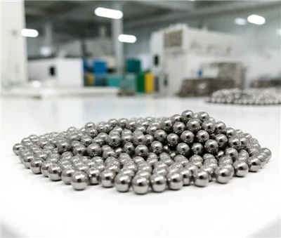

Products Introduction

Our tantalum wafers implement the manufacturing concept of "zero defect" throughout the production chain. Tantalum (Ta) is a strategic metal, and its processing difficulties lie in its extremely high melting point and easy absorption at high temperatures. To this end, we have adopted industry-leading vacuum processing technology:
Raw material screening: We only select high-quality tantalum powder with uniform particle size and very low impurities as the starting point. Through multiple vacuum electron beam melting, metal impurities such as lead, iron, and silicon, as well as non-metal impurities such as oxygen and nitrogen, are effectively removed to ensure the basic physical properties of the material.
Organization structure optimization: The internal grain size of the material directly affects the subsequent use effect. Our tantalum wafers undergo special thermomechanical processing to refine the grains, and the textures are randomized. When used as a sputtering target, this uniform microstructure can ensure a more stable atomic flow sputtered out, thereby forming an ultra-thin film with uniform thickness and few defects on the substrate.
Surface Integrity: We offer a variety of surface states for different customer needs. From economical surfaces that retain cold-rolled texture to ultra-precision polishing that reaches mirror level, ensuring a zero-gap fit with the heat sink or base during installation, optimizing thermal conductivity.
Diversity of specifications: Relying on advanced CNC cutting and grinding machine equipment, we can produce small and micro wafers with diameters ranging from 10 mm to 500 mm, and large target blanks.
Products Parameters
| Product Name | Tantalum Wafer |
| Material |
RO5200, RO5400, RO5252 (Ta-2.5W), RO5255 (Ta-10W) |
| Purity | 99.95% , 99.99% |
| Diameter | 10-500mm, customized |
| Diameter Tolerance | ±0.05mm-±0.2mm |
| Thickness | 1-20mm, customization supported |
| Thickenss Tolerance | ±0.01mm-±0.05mm |
| Surface Treatment | Polished surface, acid-washed surface, mirror surface |
Products Advantages
Unmatched corrosion resistance: Tantalum is very inert to acids, alkali, salt solutions, and organic media at room temperature, and its acid corrosion resistance is even higher than that of gold and platinum. With the exception of hydrofluoric acid (HF) and sulfur trioxide, it does not react with almost any chemical substance. This makes our tantalum wafers the "last line of defense" in the field of chemical anticorrosion, greatly prolonging the service life of expensive equipment and reducing maintenance costs.
Excellent high temperature resistance and thermodynamic properties: Its melting point is as high as 2996℃. In a vacuum environment, even at high temperatures above 1500℃, the tantalum wafer can still maintain excellent mechanical strength and shape stability. Compared with materials such as tungsten and molybdenum, tantalum has better toughness and will not become brittle after multiple thermal cycles, which greatly improves the safety of experiments and production.
Ideal biocompatibility: Tantalum is one of the few metals that can blend directly with human tissue. Our high-purity tantalum wafers do not contain any allergic or toxic impurities, and the surface is very easy to form a stable oxidation protective layer, Ta2O5. This makes it shine in the field of medical research, and can be used to make bone repair components, heart stent models, and various implantable electrodes.
Grain Control: With sputtering applications (PVD), grain size and orientation are everything. Our products have a high degree of consistency, avoiding the problem of "spray" unevenness caused by coarse grains. This means that your process window is wider and your product performance is more stable.
Products Application
Semiconductor and Microelectronics
In the manufacture of integrated circuits (IC), tantalum wafers are used as raw materials for high-purity sputtering targets to deposit diffusion barriers (Diffusion Barriers). It can effectively block the mutual penetration between copper (Cu) and silicon (Si), and is an indispensable material in the manufacture of modern high-performance CPU and memory chips.
Aerospace and vacuum technology
Due to its high melting point and low vapor pressure, tantalum wafers are widely used in the manufacture of heat shields for vacuum furnaces, heating elements, and high-temperature combustion chamber liners for jet engines. In the electronic system of artificial satellites, the raw materials of tantalum capacitors are also inseparable from such high-purity metal parts.
Health and Implants
Utilization of tantalum's non-magnetism and biological inertia in medical institutions. Tantalum wafers can be precision machined into cranium repair pieces and broken bone joints, and are completely safe and undisturbed even in nuclear magnetic resonance (MRI) environments.
Chemistry and Energy
It is used to manufacture the inner lining cover plate of the strong acid reaction kettle, the heat exchanger seal, and the electrode catalyst support body of the fuel cell. The reliability of tantalum wafers is irreplaceable when dealing with strong corrosive media such as hydrochloric acid and sulfuric acid.
Superconductivity and Frontier Physics
In quantum computing and superconducting research, tantalum, as a metal with a high superconducting critical temperature, is often processed into thin film substrates or coupling components with specific shapes.
Contact Us
We have mature batch supply capabilities, and can purchase small batches for small and medium-sized enterprises, and large-scale order needs of large enterprises.
We can provide exclusive quotation discounts for batch purchases. Relying on an efficient supply chain to ensure fast delivery of orders.
So if you need a Tantalum Wafer, then contact us now to get the latest quotation.
Phone Number
(86)-18291772322
Ta-Nb@titanmsgp.com

Hot Tags: tantalum wafer, China tantalum wafer manufacturers, suppliers, factory