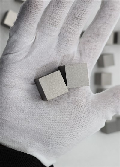

Niobium Round Disc

Our Niobium Round Discs/Wafers are refined from high-quality high-purity niobium ingots (EB Melted Ingots) by cold rolling, precision stamping/wire cutting and high vacuum bright annealing. The surface can be provided in a variety of states such as Mirror Polished, Bright Rolled or Pickled.
With extremely low vacuum outgassing rate, excellent corrosion resistance, high melting point (2468 ℃) and excellent superconducting transition characteristics, our niobium wafers are widely used in semiconductor thin film deposition, PVD sputtering target blank, superconducting cavity (SRF Cavity) manufacturing, medical implant casing and high temperature chemical anticorrosion fields.
I. Why Choose Our Niobium Discs?
1. Ultra-Smooth Surface Finish
The real disc (as shown in the product picture) presents a mirror-like metallic luster, and the surface is free of scratches, oxidized colors, and scallops. The extremely low surface roughness (Ra ≤ 0.08 µm) can significantly reduce the defects during film deposition and improve the uniformity and adhesion of the coating.
2. Strictly control gas impurities and dense crystallization (Low Outgassing & Uniform Grain)
Through multiple electron beam (EB) vacuum melting and fine annealing, interstitial impurities such as oxygen (O), nitrogen (N), and hydrogen (H) are strictly controlled, and the grain size is uniform to ensure that in ultra-high vacuum (UHV) and extremely low temperature There is no brittle cracking in the temperature, and it has excellent vacuum degassing performance.
3. Excellent Corrosion Resistance and Anodizing coloring
Niobium exhibits strong chemical inert to most acids (such as hydrochloric acid, nitric acid, and aqua king) at room temperature. At the same time, niobium wafers can present colorful oxide film colors (blue, gold, purple, etc.) after anodizing, very suitable for high-end jewelry, anti-corrosion components and electrode materials.
4. Flexible customization capabilities (100% Customized Capabilities)
We support customization according to the buyer's engineering drawings (CAD/STEP files), including special-shaped drilling, stepped groove processing, Chamfering, and specific particle size control.
II. Technical Specifications Table
1. Basic Properties Property Item
| Property | Value | Notes |
| Grade | R04200 (Unalloyed Nb, EB Melted) R04210 (Unalloyed Nb, Vacuum Arc Cast) Nb1/Nb2 (national standard) | Conforms to ASTM B393/B392 and other international norms |
| Purity | Purity ≥ 99.95% (99.99% ultra-high Purity grade can also be provided) | Low gas impurities (O, N, H, C) control |
| Density | 8.57 g/cm³ | Density up to 99.9% or more |
| Melting Point | 2468 ℃ | Excellent high temperature deformation resistance |
| Boiling Point | 4744 ℃ | Strong stability in high vacuum circumstances |
| Superconducting Transition Temperature (Tc) | 9.25 K | Higher critical temperature in elemental superconductors |
| Elasticity Modulus | 105 GPa | Good plasticity and ductility |
2. Chemical Composition (Max wt%)
| Element | Nb (purity) | Ta | Fe | C | Ni | O | N | C | H |
| R04200 | Bal. (≥99.95%) | ≤ 0.10% | ≤ 0.005% | ≤ 0.005% | ≤ 0.002% | ≤ 0.015% | ≤ 0.010% | ≤ 0.005% | ≤ 0.0015% |
| High Purity | Bal. (≥99.99%) | ≤ 0.01% | ≤ 0.001% | ≤ 0.001% | ≤ 0.001% | ≤ 0.005% | ≤ 0.003% | ≤ 0.002% | ≤ 0.0005% |
3. Dimensions & Processing Item Specification
| Item | Specification |
| Diameter | φ 10 mm –φ 300 mm (large size can be customized according to drawings) |
| Thickness | 0.1 mm – 20 mm etc |
| Tolerance | Diameter Tolerance: ± 0. 05 mm; Thickness tolerance: ± 0. 01 mm (precision grade) |
| Technology | Electron Beam Melting (EB Melting) > Forging/Slab > Cold Rolling > Vacuum Annealing > Precision Stamping/Water Jet/Turning > Polishing |
| Supply State | M (soft/fully annealed), Y (hard/cold hardened) |
| Surface Finish | Mirror polished (Ra ≤ 0.08 µ m), bright surface, acid wash, sandblasted surface |
| Standards | ASTM B393 (Standard Specification for Niobium and Niobium Alloy Strip, Sheet, and Plate) ASTM B392, ISO 9001: 2015 |
III. Typical Application Areas (Primary Applications)
Semiconductor & Thin Film Deposition: As a Sputtering Target Blank or Substrate, it is used in microelectronics, optical coating and flat panel display production.
Superconducting Research and High Energy Physics (Superconductivity & Particle Physics): Used to manufacture substrates for superconducting radio (SRF) resonant cavity components and superconducting quantum computer devices.
Chemical Processing & Electrochemistry: Valve gaskets, reactor seals and anode protection electrodes resistant to strong acid corrosion.
Medical Devices: Due to its good biocompatibility, it is used in medical implant enclosures and human bone plate components.
Capacitors & Electronics: High-purity niobium anode substrate materials in solid-state Capacitors.
IV. Packaging and Inspection
Inspection: Each batch of products is provided with an original Quality Inspection certificate (MTC-Material Test Report) that complies with EN 10204 3.1, including complete chemical composition analysis (MIT) and mechanical property test data.
Protective Packaging (Packaging): Each niobium wafer is wrapped with dust-free protective film/paper, and is packaged in vacuum-sealed plastic bags or special shockproof boxes, and the exterior is reinforced with wooden boxes/hard cartons to ensure zero scratches and zero oxidation during sea and air transportation.
Our products


Packing


Delivery


Our factory & equipment



Hot Tags: niobium round disc, China niobium round disc manufacturers, suppliers, factory